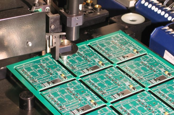
Your Professional PCB Design Team!
PCB Design Service
Tell Me More

Services

Our PCB layout electronic design services: New Product Development, Engineering Changes, Reverse Engineering, Cost Reductions, Validation & Verification and Quick Turn electronic design prototypes.


Low Complexity

Mid Complexity

High Complexity

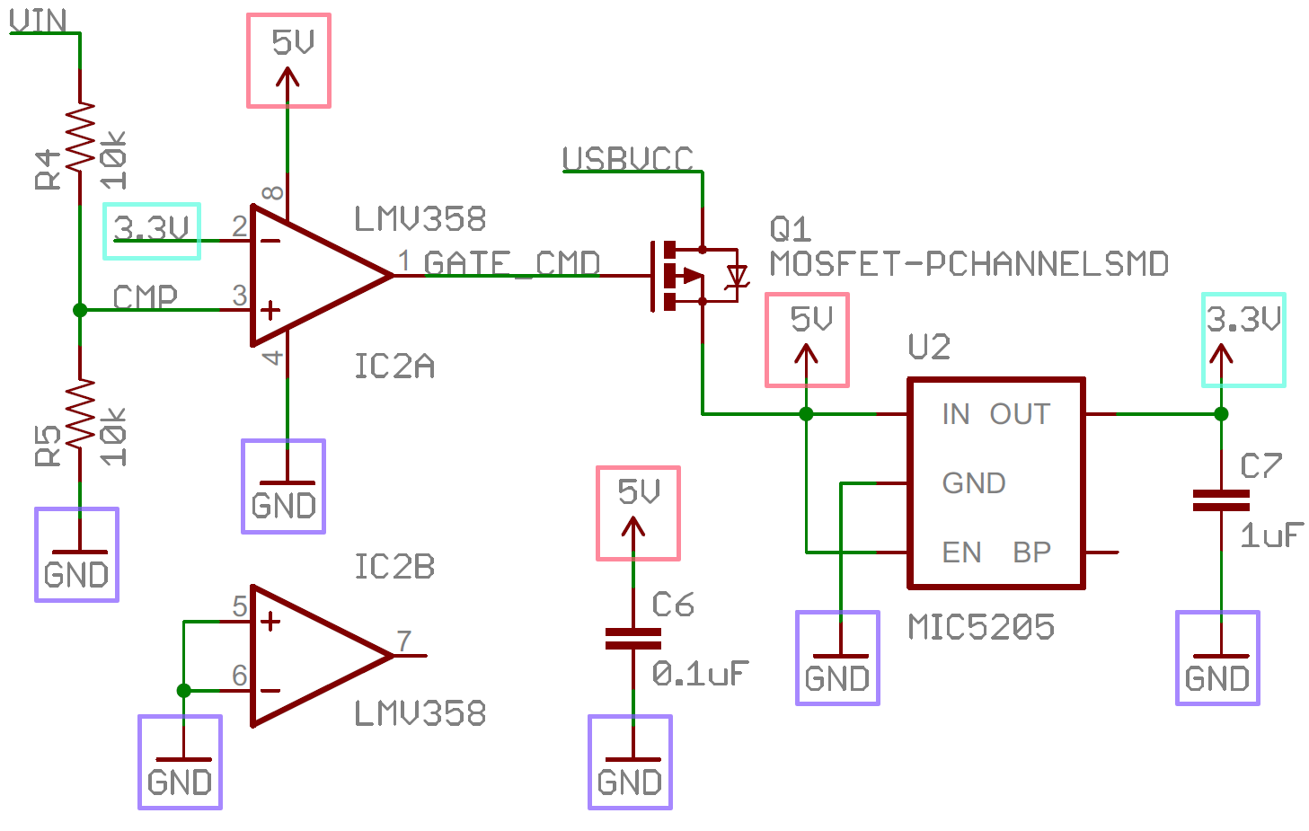
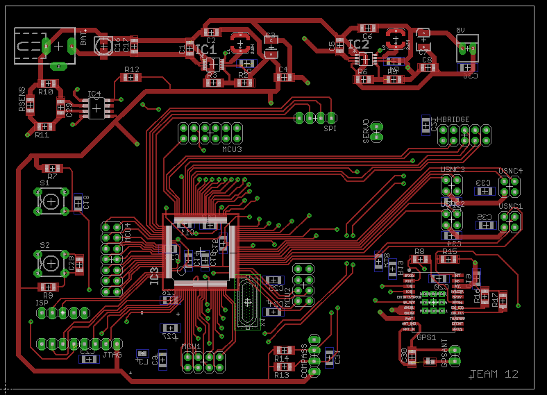
Our PCB layout electronic design capabilities: Single layer, Double layer, Multilayer, Flexible, High-speed, Impedance controlled, Radio Frequency RF, Ground-Power planes, Backplanes, Thru-hole, SMT and Mixed technology.


Development Workflow

The typical PCB layout electronic design tools that we use include Pads, Orcad, Allegro, Altium and CAM350 and we take extreme care in the selection, planning and design of grids, tracks, pads, vias, annular rings, layers, polygons, clearances, placement, routing, silkscreen, solder mask, keep outs, test points, power planes, grounding, panelization, fiducial marks, mounting holes, cut-outs, material, thermal reliefs, footprints and libraries.

Our PCB layout electronic design methodology mitigates the typical harmful effects of crosstalk, induction, attenuation, impedance, delays, reflection and ground loops.


Professional Schematic Entry

Schematic Entry

Professional Layout Design

Layout Design

Let's us be of help
Gerber Output Files

Gerber Output Files

Let's work togheter